Molybdenum, a refractory metal with exceptional thermal and electrical properties, has become indispensable in the electronics and semiconductor industries. Its high melting point, low thermal expansion, and excellent corrosion resistance enable critical processes from chip fabrication to power device packaging. This article examines the key applications of molybdenum in these sectors, providing engineers and procurement professionals with the technical data needed to evaluate its suitability for their specific requirements. As a trusted supplier of high-purity molybdenum products, Better Metal delivers precision components that meet the strictest industry standards.
Semiconductor manufacturing involves extreme temperatures, reactive gases, and stringent purity requirements. Molybdenum's unique combination of properties addresses these challenges:
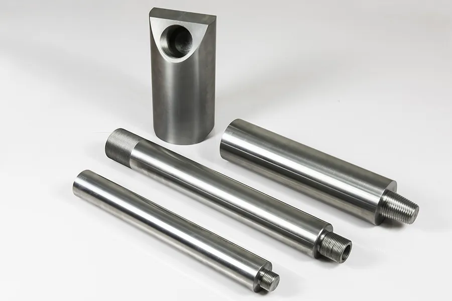
Ion implanters require components that can withstand high-temperature plasma environments while delivering consistent dopant ions. Molybdenum is the preferred material for arc chambers, repeller plates, and extraction electrodes. Its low sputter yield improves source lifetime and reduces particulate contamination, crucial for advanced nodes below 7nm. Better Metal supplies custom-machined molybdenum parts with controlled grain structure for uniform erosion.
Molybdenum sputtering targets are widely used to deposit Mo layers in TFT-LCD displays, thin-film solar cells, and barrier/seed layers in semiconductor metallization. Key advantages include:
Compared to alternative materials like tungsten and titanium, molybdenum offers a superior balance of low resistivity and etch selectivity, making it essential for applications such as gate electrodes in CMOS logic devices.
With power densities rising in high-performance computing and RF devices, effective heat dissipation is critical. Molybdenum-copper (MoCu) composites provide tailored thermal expansion matching to ceramics and semiconductors while offering high thermal conductivity (180–250 W/m·K). These are used in heat sinks, baseplates for IGBT modules, and lid materials for hermetic packages. Alternatively, pure molybdenum is employed as heat spreaders for high-power laser diodes and LED packages.
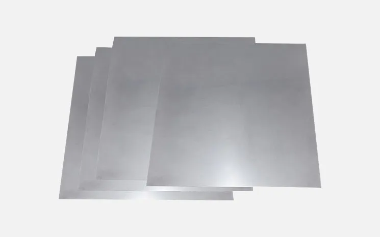
Semiconductor furnaces rely on molybdenum heating elements, reflectors, and supports due to their resistance to thermal cycling and oxidation at up to 1700°C. Molybdenum shields improve temperature uniformity and energy efficiency in diffusion and LPCVD processes. Better Metal's hot-rolled molybdenum sheet provides consistent emissivity and long service life.
When selecting materials for semiconductor applications, engineers often compare molybdenum with tungsten, tantalum, and nickel-based alloys. The following points highlight molybdenum's competitive edge:
Better Metal has supplied high-performance molybdenum products to leading semiconductor equipment manufacturers for over a decade. Our quality management system includes:
We offer standard stock sizes for common applications, as well as rapid prototyping services for R&D projects. Whether you require sputtering targets, ion source parts, or thermal management components, our technical team assists with material specification and geometry optimization.
Molybdenum continues to play a vital role in advancing semiconductor technology, from enabling smaller feature sizes to managing higher power densities. Its exceptional thermal, electrical, and mechanical properties provide reliable performance across multiple process steps. For organizations seeking a trusted material supplier with proven expertise in the electronics industry, Better Metal offers precision molybdenum solutions backed by rigorous quality control and responsive customer support. Contact our engineers to discuss your application requirements.
Share this page
If you have any product needs or questions, please leave us a message for consultation.
TEL: 86-18623759992
jason@bettmetal.com

Innovating Materials
for a Brighter Future